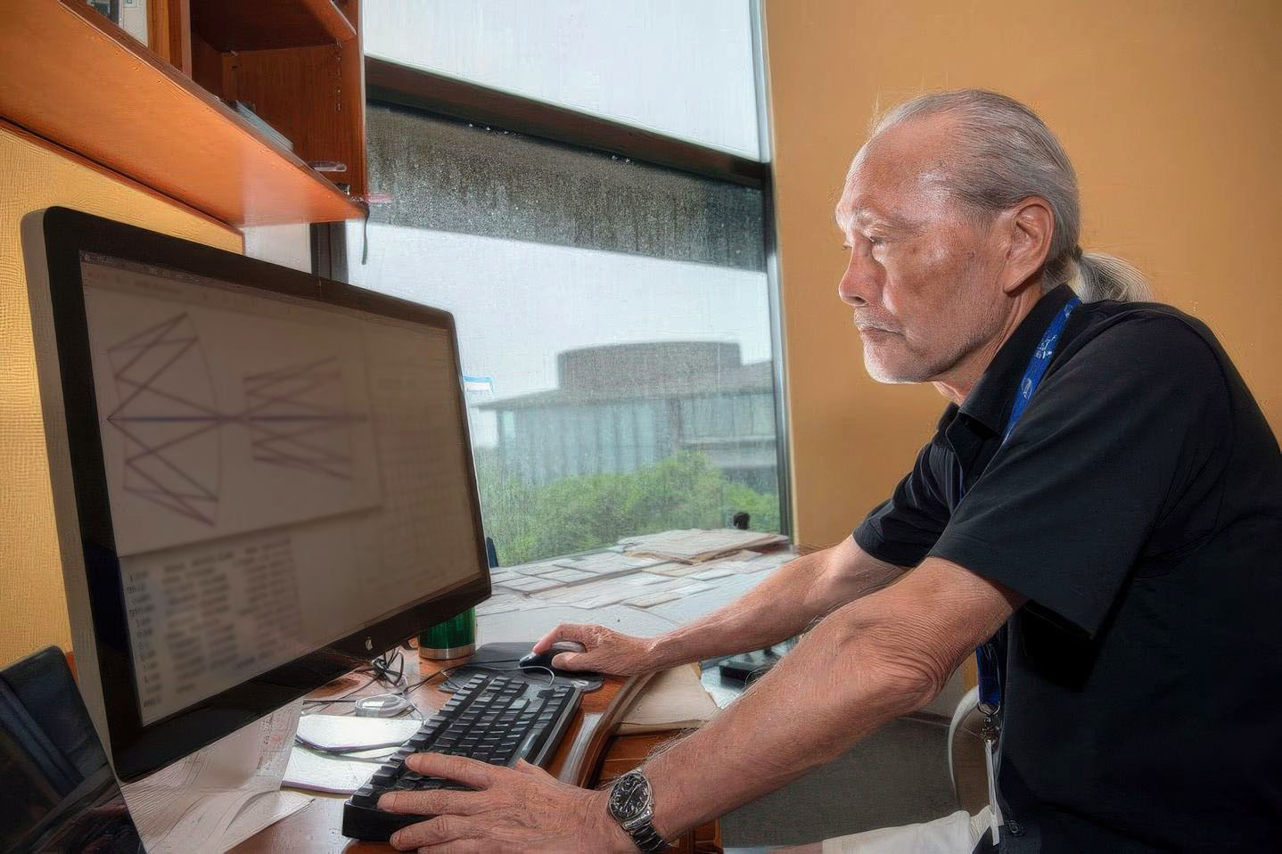
image: Professor Shintake uses OpTaliX, an optical simulation system, to figure out the precise placement and angles of mirrors for his EUV lithography optical system design.
OIST Professor Tsumoru Shintake has developed a groundbreaking new approach to semiconductor chipmaking that could make future computer chips smaller, faster, more energy efficient, and significantly less expensive to manufacture.
Published on June 12 in the Journal of Micro/Nanopatterning, Materials, and Metrology (JM3), Professor Shintake’s latest research introduces a radically redesigned optical system for high numerical aperture (high-NA) extreme ultraviolet (EUV) lithography—the advanced technology used to print the microscopic circuits found in today’s most sophisticated semiconductor chips.
For decades, scientists have sought ways to improve EUV lithography, but current systems remain extraordinarily complex and expensive, with individual machines costing hundreds of millions of euros. Through years of research, modeling, and simulation, Professor Shintake developed an innovative optical design that simplifies the system while preserving exceptional precision. His simulations indicate the new approach could produce circuit features as small as 2–3 nanometers, while reducing the cost of next-generation chipmaking equipment to a fraction of today’s machines.
“Current EUV lithography systems cost hundreds of millions of euros per machine,” said Professor Shintake. “My new design should achieve fine 2–3 nanometer-scale details in a much cheaper way compared to today’s state-of-the-art machines.”
The potential impact of Professor Shintake’s work extends far beyond semiconductor manufacturing. As artificial intelligence continues to drive demand for computing power, the International Energy Agency predicts that electricity consumption from data centers will double by 2030. By enabling denser semiconductor chips with shorter signal pathways, Professor Shintake’s design could reduce energy loss, generate less heat, and significantly lower the power required for both computing and cooling.
“Our design has the potential to make high-NA lithography much simpler and more affordable,” Professor Shintake explained. “By achieving finer chip designs, we can create higher-density memory and more efficient logic chips. This technology could have transformative impacts on society by powering the future of AI while making electronics faster, more energy efficient, and less expensive to operate.”
The breakthrough is the result of years of painstaking research. Professor Shintake explored new ways of arranging multiple mirrors within the lithography system, ultimately discovering a configuration that can cancel optical distortions while maintaining the high numerical aperture needed to produce increasingly tiny circuit patterns.
The next step is turning the concept into reality. Professor Shintake and his team have already begun developing a physical prototype of the new EUV lithography system with the goal of creating lower-cost, high-performance manufacturing technology for the semiconductor industry.
Professor Shintake’s research exemplifies the bold, interdisciplinary innovation taking place at OIST. By tackling one of the world’s most complex engineering challenges, his work has the potential to transform semiconductor manufacturing and help power the next generation of artificial intelligence, computing, and countless technologies that improve lives around the world.